System Block Diagram
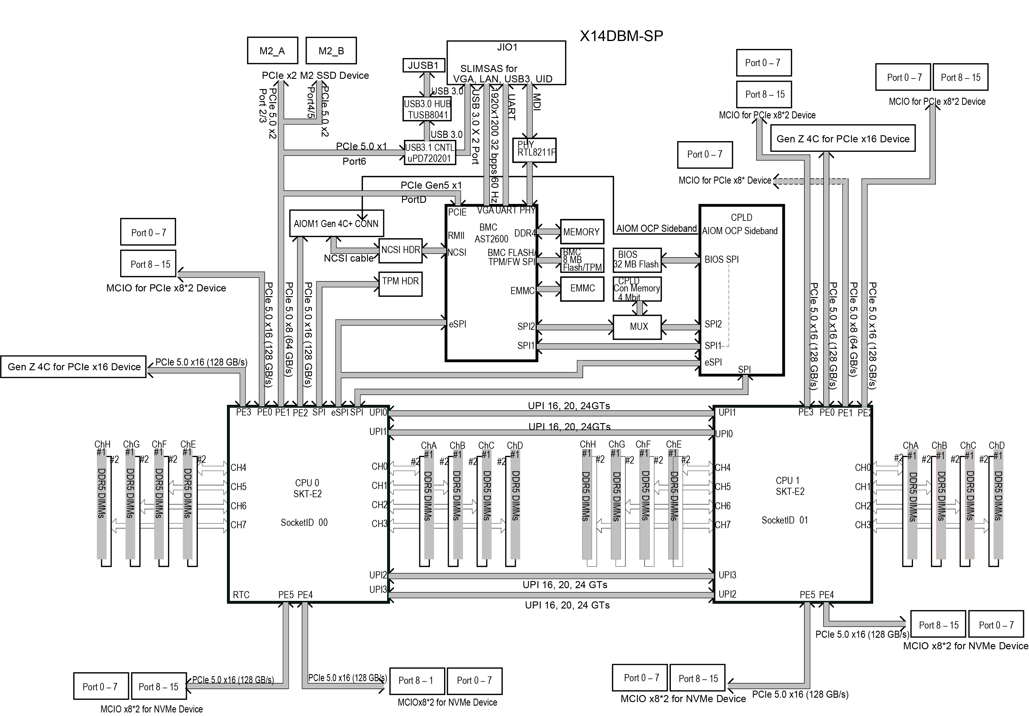
Figure 5. System Block Diagram
System PCIe Lane Distribution
|
SYS-122H-TN PCIe Lane Distribution |
||||
|---|---|---|---|---|
|
CPU |
Port |
PCIe |
Motherboard Connector |
PCIe Lane Assignment |
|
CPU0 |
PE0 |
x8 |
JPCIE2A1 |
Not Used |
|
x8 |
JPCIE2B1 |
Not Used |
||
|
PE1 |
x81 |
M.2-C1 (x2), M.2-C2 (x2) |
Internal 2x NVMe M.2 Slots |
|
|
PE2 |
x16 |
JAIOM1 |
AIOM/OCP 3.0 NIC Slot A1 |
|
|
PE3 |
x16 |
JPCIE1 |
PCIe Expansion Slot 2 |
|
|
PE4 |
x8 |
P1_NVME0 |
Not Used |
|
|
x8 |
P1_NVME1 |
Not Used |
||
|
PE5 |
x8 |
P1_NVME2 |
NVMe Drive Bays 0,1 |
|
|
x8 |
P1_NVME3 |
NVMe Drive Bays 2,3 |
||
|
CPU1 |
PE0 |
x16 |
JPCIE5 |
PCIe Expansion Slot 1 |
|
PE1 |
x8 |
JPCIE3A1 |
Not Used |
|
|
PE2 |
x8 |
JPCIE6A1 |
NVMe Drive Bays 4,5 | |
|
x8 |
JPCIE6B1 |
NVMe Drive Bays 6,7 |
||
|
PE3 |
x8 |
JPCIE4A1 |
PCIe Expansion Slot 3 |
|
|
x8 |
JPCIE4B1 |
|||
|
PE4 |
x8 |
P2_NVME0 |
NVMe Drive Bays 8,9 |
|
|
x8 |
P2_NVME1 |
Not Used |
||
|
PE5 |
x8 |
P2_NVME2 |
Not Used |
|
|
x8 |
P2_NVME3 |
NVMe Drive Bays 10,11 |
||
1Some PCIe lanes from this port are routed directly to onboard devices (USB controller & BMC)